
|
|||
|
|||
|
|||
|
Technology Via-in Pad Via-in-pad technology is becoming a more essential strategy used to support finer pitch devices. It is used to open up routing channels on the surface of the board. Many BGA substrates and PCBs that received BGAs use "dog-bone" design to accommodate the need for PTHs and pads to accept the solder balls. As show in Figure A, this can be much more efficiently routed using via-in-pad. Holes are drilled into the center of the SMT pad and then plated, filled with a thermal set epoxy based material, to provide a smooth surface.
Figure A
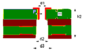
Back-drilling Vias Back drilling technique is used to enhance the electrical property for high frequency applications. This is achieved by cutting away the metallized surface of the via wall from the backside of the board leaving a conductive structure that penetrates from the top surface only partway through the hole (Figure B.). By back drilling the via, the launch impedance is improved by reducing via capacitance and more importantly the launch resonance effect is mitigated.
Figure B
|